

1D nextnano
1D nextnano3 Tool
Next Generation Nanodevice Simulaton
Fabio Compagnone, I-CODE s.r.l.
Welcome to the 1D version of the next generation 3D nanodevice simulator: nextnano3 QUANTUM!
We would like to thank the nextnano3 Development Staff in the Walter Schottky Intitüt, TUM (Germany), and OPTOLAB, in University of Rome Tor Vergata (Italy) for their collaboration. In particular we acknowledge Dr. Stefan Birner, Dr. Michael Povolotskyi and Dr. Fabio Sacconi for their precious help.
In the following you will learn how to use the tool and how to design your device structure and run the simulations. For now on, Client is the computer where you are running the browser (your local computer) while Server is the computer where you are connected (I-CODE server). This document is not intended to give a detailed overview of the simulator, which can be found in the nextnano3 website, but it would give all the information needed to the user to easily set up a device and run the simulation. In the text pay particular attention to red text warnings, because these are considered critical points, being the major sources of possible errors.
nextnano3 is powerful simulation code developed at TU-Munich, in collaboration with many other university and company researchers (some of them are from Roma Tor Vergata), to simulate nanoelectronic devices, quantum dots, quantum wires, RTD's, MOSFET's, HEMT's, diodes etc. The main features of this simulator are*:
- includes group IV materials (Si, Ge, SiGe) and all III-V materials and its ternaries as well as lattice-matched quaternaries
- flexible structures and geometries
- fully quantum mechanically
- based on the 8-band k.p model within a high precision finite differences grid
- includes strain in layered pseudomorphic structures from lattice mismatch
- includes piezo and pyroelectric charges
- growth directions along [001], [011], [111], [211], ... in short along any crystallographic direction
- equilibrium and non-equilibrium
- calculation of current close to equilibrium (semi-classical)
- magnetic field
- 1D, 2D** and 3D**
* this information is taken from the nextnano3 web site
** Currently only the 1 Dimension version of the simulator is available for the ICODE users.
The detailed manual for the nextnano3 input file can be found here.
The GUI (Graphical User Interface) is realized as a Java applet, and we tried to make it easy to use. It is still under development, and suggestions will be welcome for its improvement. We remind the users that, as general rule, when a new version of the GUI is released, the old Projects (saved in the serialized .ser files) can be read only by the old applet version, and not by the new one. On the other hand it is almost always possible to run the simulations using the old input files. It must be noticed that if we upgrade simulator code to a new release (for instance to correct some major bugs), there is an high possibility that the old input files must be corrected or converted (we'll try to provide such converters in short time).
There are 6 simple steps to follow for a complete device simulations:
- Login
- Select working directory
- Run the nextnano3 simulation tool
- Use the device editor
- Monitoring the job execution
- Plot the results
Step 1 & Step 2: Login and Select working directory
For the first two steps see the detailed instructions in the documentation file: Accessing ICODE system.
Step 3: Run the nextnano3 Simulation Tool
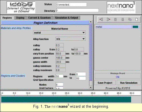
By having selected a well defined working directory you can now run the simulation tool. Click on the nextnano3 icon and a window like that in Fig. 1 will appear.
|
The applet is divided in four different frames. |
|
In the top frame you can find the usual general fields status, which tells you if the connection client/server is established, and the working Directory. If the Status is disconnected you cannot save your Project or run your simulation. |
|
|
The central frame is used to define the properties of your device and your simulation. It is divided is four sections: Regions, Doping, Current & Quantum and Simulation & Output.The left and the bottom frames are devoted to the device definition. In the left frame you can find an editor which can be used to build a device piling up segment of different materials. |
|
| The thickness and the properties of each material can be defined in the central frame. In the bottom frame you can see a schematic representation of the one-dimensional device. In the left frame you can find also the Message Board, to give you warnings and hints, and the Save Project and Run Simulation buttons |
There are two ways to run the wizard:
- You edit directly the input file with the text editor. In order to properly generate a working input file you may need to read the nextnano3 web pages. This way is much more complicated with respect to the following one however it allows you to use nextnano3 for very complicated situations.
- You can use the GUI as discussed in the following
Step 4: Use the Device Editor
If you would avoid entering the device structure directly in the nextnano3 input file you can use the GUI wizard.
|
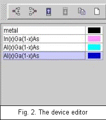
In the left frame of the applet you can find the device editor. It is the totally interactive tool which let you “build” the device piling-up different materials as “bricks”, each one representing a section of the device (namely a region). Each region can be associated to various characteristics, like the type of material, thickness, doping, and even a customizable color. |
|
The functions of the buttons at the top of the frame are the followings (from left to right): add a new region, delete a region, move up/down a selected region, copy a selected region at the bottom of the structure. A random color is associated to a new region, but it can be changed simply clicking the respective color and selecting a new one on the colors table. |
|
|
The structure of the whole device is plotted schematically in the bottom frame of the applet. Here, from left to right, the different regions are represented in scale, and the ruler gives thedimensions in nanometers (see Fig. 2). Each region can be selected in one of the two representations and edited, changing its characteristics. |
To complete the definition of your device you need to specify the characteristics of each layer in the Regions and Doping sections. Having the layer selected in the left structure click on the region label in the central frame of the interface. Associated to each layer must be defined:
-
the material type, selecting the name in a list of available materials
-
if it is an alloy you can select the appropriate alloy function and the value of the component concentration
-
the thickness of the region, width, (automatically the tool gives its initial and final position in the corresponding fields)
-
number of nodes and grid factor, to specify the characteristic of the 1D grid used to perform the calculations
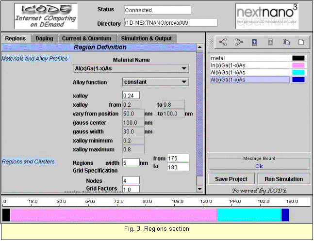
In this example we started to build a device with a metal contact layer of 5 nm (black), then we added three regions of AlGaAs, identified with different colours accounting for different characteristics (alloy concentration, doping, etc.)
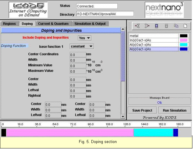
As default a material IS DOPED, but you can change this conditions selecting the layer and accessing the Doping section with a click on its label. Here you can set the include doping variable to yes/no. Then you can choose the doping function, which can be simple (costant, i.e. uniform doping in one or more regions) or non uniform profile (gaussian, step, well, etc.). Then you must provide the coordinates of the doped region, depending on the doping function selected. The impurity parameters are also needed in input, i.e. if there are acceptors or donors, the number of energy levels which must be considered as well their position respect to the conduction or valence band. The value of the doping concentration must be given in units of 1018 cm-3.
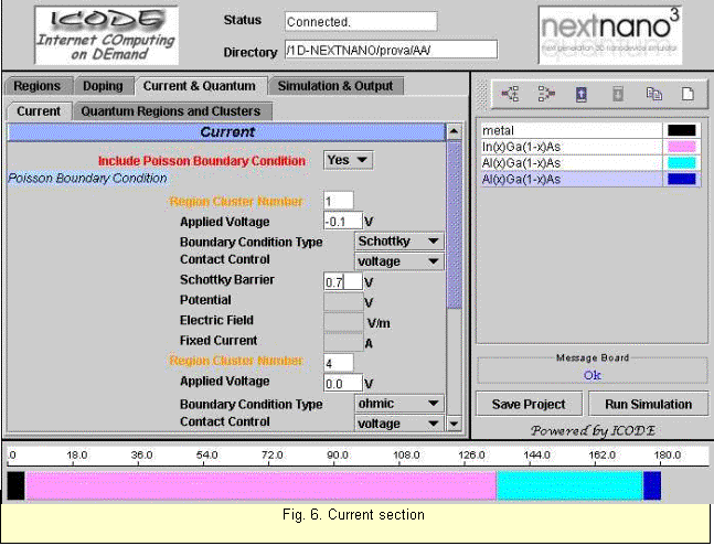
The next section, namely Current, is used to define which type of equtions are going to be solved inside the device. If current calculation is needed, you have to set the variable Poisson Boundary Condition to yes. The 1D device has two contact by default: the first and the last layer, which are automatically selected in the tool. For both you have to specify either the type of contact or the boundary condition you want (Schottky, Ohmic, Dirichlet, Von Neumann, etc.). Thus, depending on this choice, you must provide the information on the required physical parameters, such as the applied voltage, the Schottky Barrier, etc. Please note that the selection of the boundary condition/contact type can exclude some of the parameters.
Very important! Please remember that the two contact regions must be defined as independent layers in the device, and are not considered for the calculation (i.e. no equation will be solved in these boundary regions). Our suggestion is to add always two small metal layers at the beginning and the end of the device, if ohmic or schottky contacts are needed. See nextnano3 Poisson Boundary Condition section for details.
Also here you can set up the simulation with a variable applied voltage. For the Voltage Sweep you must provide the number of steps and the step voltage increment. You are strongly encouraged to visit the nextnano3 site, to study their tutorials, which is the best way to learn how to use such functionalities.
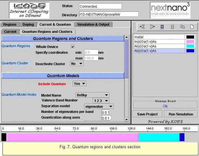
In the section Quantum Regions and Clusters you can decide to include or not quantistic calculation for your device, setting the variable Include Quantum.
The definition of a quantum region, i.e. the region of the device in which quantistic calculations will be performed, is very important. You have different choices: you can select the whole device or provide initial and final coordinates. In the same section you need to select the Quantum Model to use in the calculations (effective mass, 8x8 K·P, 6x6 K·P, classical), the number of valence and conduction bands (Very important: this parameter must be considered as the maximum number of eigenvalues calculated in the simulation! Afterwards you can define the energy range for the eigenvalues which will be in the output, see the Output section), the boundary conditions in the main directions, and many other features for both holes and electrons. A useful hint to reduce the computational time is to perform initially a classical calculation, identifying the region where quantistic calculations are necessary (the ones with the highest carrier density).
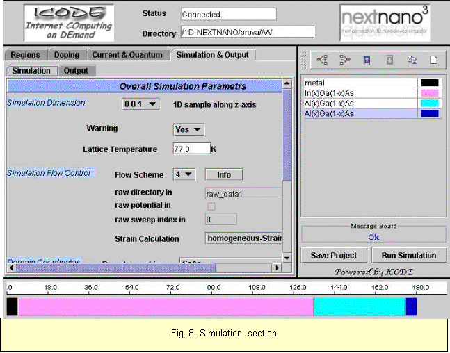
The physical parameter for the simulation are defined in the following section Simulation. The most important features here are the Simulation Direction, the Lattice Temperature, and the Strain properties. Also here you can choose to use unusual 'strange' orientation of your axis, for wurtzite and zincblende structures. If you need warnings from the program during the simulation remember to set the specific variable. Here you can also define the Flow Scheme of the simulation. Different numbers correspond to different complexity of calculation. The complete information on all the possible flow schemes are given in the nextnano3 web pages, see the Flow-Scheme section.
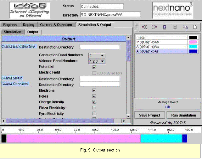
In the last section Output you can specify all the quantities you would like to have in the output files, simply selecting or unselecting the corresponding flag. By default the generated output files are saved in the working directory. If you need the output files to be stored in a different destination directory you must provide the name here (Very important: the
directory must exist!). If some outputs are not compatible with the selected model or flow scheme you will be warned during the simulation.
Once you have defined the device and the physical and numerical condition for the simulation you can access the submit the request for the simulation, or to save the input file without starting the simulation.
You can at this point save the profile of the project (Save Project). In this way you create the file .ser in your directory. This file contains all your setting of the device (all the project) and can be run directly by pressing with the mouse the start button. In this way you can easily modify your project later on.
When nextnano start the simulation, it reads the file device.in. When you submit the job (Run Simulation button) you can create this input file according to your device definition if the create input file is chosen. Otherwise you can use another (for example manually modified) device.in input file present in the working directory if use old input file is selected.
Step 5: Monitoring the job execution
After the job has been submitted you can monitor the job execution by clicking on the Jobs Status link in the left frame, just above the list of the Services (simulators). For details on this see the relative documentation: Job Monitor Utility.
Step 6: Plot
Results of the simulation can be either downloaded on the CLIENT computer or plotted using the ICODE Hyperplotter tool. For reference see the relative documentaton file: Hyperplotter Graphic Utility.