

Tiber-1D
Tight-Binding Evolutionary CAD –1D
Aldo Di Carlo , University of Rome Tor Vergata
Welcome to the Tight-Binding Evolutionary Cad (TIBER-1D) software !!
This software allows you to calculate electronic and optical properties of heterostructures where the translational symmetry is broken in the [001] direction, such as Quantum Well grown on the [001] oriented substrate.
With the TIBER-1D software it is possible to calculate
- Energy levels of a quantum well
- Band dispersion in the parallel plane ([1,0] and [1,1])
- Intraband and interband TE and TM absorption coefficient
INTRODUCTION
- LOGIN
- Select working directory
- Description of TIBER-1D interface on ICODE
- Monitoring the job execution
- Plot the results
The TIBER project consist in a microscopic description of nanostructure obtained by using state of art Empirical Tight-Binding method. Up to now only the 1D version has been released which allow for the description of Quantum Well systems. A full 3D version in almost ready al will be available on line in the near future.
In the following we will present the graphical interface to TIBER-1D. A comprehensive introduction to Empirical Tight-Binding modelling can be found in
Aldo Di Carlo
Microscopic theory of nanostructured semiconductor devices: beyond the envelope-function approximation
Semiconductor Science and Technology 18, R1-R31 (2003)
Step 1 & Step 2: Login and Select working directory
For the first two steps see the detailed instructions in the documentation file: Accessing ICODE system.
3: Description of Tiber-1d Simulation interface on icode
There are two ways to run the wizard:
- You edit directly the input file with the text editor.
- You can use the GUI as discussed in the following.
By having selected a well defined working directory you can now run the simulation tool. After clicking the TIBER-1D icon, a new window will pop-up with the program interface.
|
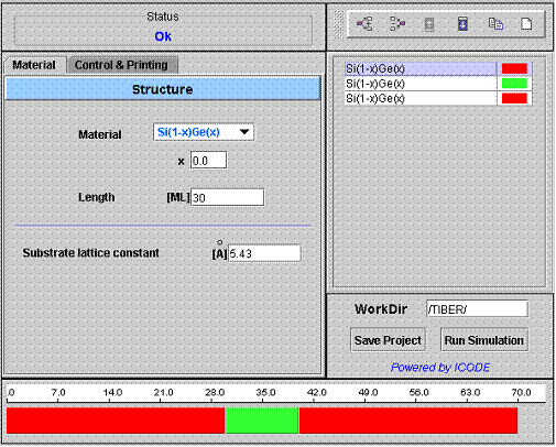
In the right frame of the applet you can find the device editor. It is the totally interactive tool which let you build
the device piling-up different materials as blocks, each one
representing a section of the device. By clicking of the block one can
define (left panel) the block structue (type of material, composition
and length). |
|
|
Fig.1. The TIBER-1D interface |
Left frame.
Contains two panels. In the Material panel you can define the structure of the heterojunction while in Control & Printing you can define parameters for the calculation such as number of levels etc. etc. In upper part of the left frame you can find also information about the Working Directory (WorkDir) and the status of the connection to ICODE server.
Right frame.
Shows the layer sequence of the simulated structure. Each layer has a well define structure (material, composition and lenght). By clicking on the layer the left panel will show the block structure.
MATERIAL PANEL
Here (see Fig 1) you can chose the material of the block (= sequence of equal layers), the alloy composition x, and the length of the block in units of Monolayers (ML). A monolayer is composed of two atomic planes (1ML = lattice constant / 2 for non strained layers).
The Substrate lattice constant define the lattice constant of the substrate where you are grooving you nanostructure. All your nanostructure s pseudomorphically strained on this lattice constant.
CONTROL AND PRINTING PANEL
|
The Control and Printing panel is divided in three sections: Energy, Type of Calculation (Dispersion or Optics) and Control. | ||||
|
|
|||||
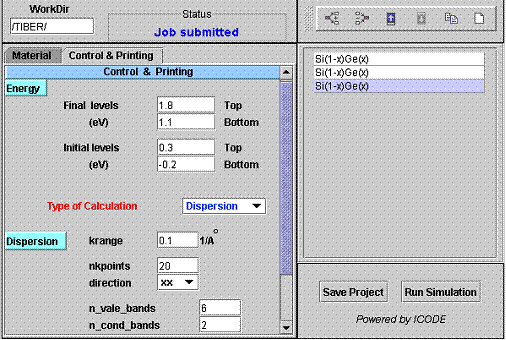
The Energy section define the energy windows where the electronic and optical properties of the nanostructure will be calculated. Two energy windows can be defined:
- Initial Levels: with energy (E) in the rangeE_bottom < E < E_top
- Final Levels: with energy (E) in the rangeE_bottom < E < E_top
We have used two different windows because this is will help in defining optical properties of the system where, for example, initial level could be valence band and final level the conduction band.
The only requirement here is that E(initial levels) < E(final levels). The energy windows represent hard limits. Very important ! Energy level outside these windows will not be calculated.
TYPE OF CALCULATIONS
When the Dispersion mode is select, the band structure of the nanostructure in the parallel space (in-plane space) will be calculated.
|
krange
|
Maximum value of the k vector for the band dispersion calculation. Units = 1/Angstrom (remember that end of the Brillouine zone is 2pi/a with a = lattice constant) |
|
nkpoints
|
Number of k points considered in the calculation |
|
direction
|
xx = dispersion along the line [100], xy = dispersion along the line [110] |
|
n_vale_bands
|
Number of initial bands that will be plotted in output |
|
n_cond_bands
|
Number of final bands that will be plotted in output |
The output of this calculation will be:
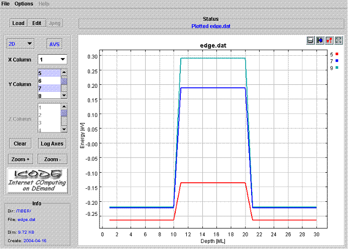
edge.dat, which contains the band energy [eV] profile at Gamma point (K=0) as a function of depth (unit: MonoLayer=2 atomic planes). The format is:
|
depth
|
E(8th valence band)
|
E(7th valence band)
|
...
|
E(1st valence band )
|
E(1st conduction band)
|
...
|
E(12th conduction band)
|
See figure 3 for a plot of the band edge. The picture shows the strained valence band profile of a Si/Si0.5Ge0.5/Si quantum well. Heavy hole, Light Hole and Spin orbit hole are shown.
|
|
Fig.3. Plot of the edge.dat file. |
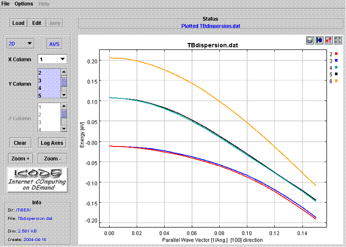
TBdispersion.dat, which contain the band dispersion [eV] in the following format
|
k_value_1
|
E(n_vale_bands)
|
E(n_vale_bands-1)
|
...
|
E(n_cond_bands-1)
|
E(n_cond_bands)
|
Dispersion are calculated within the energy windows defined above. Thus if, for instance, we ask to calculate 6 initial bands but during the calculation one of these bands has energy outside the energy windows, that band will not be calculated !! A detailed tailor of the energy windows is necessary. Figure 4 shows a plot of the TBdispersion.dat file. The picture shows the first 6 valence subbands of the strained Si/Si0.5Ge0.5/Si quantum well of Fig. 3.Spin splitting is very small.
|
|
Fig.4. Plot of the TBdispersion.dat file. |
When the Optics mode is select, the absorption coefficient between the initial level and the final levels will be calculated for both TE and TM polarization of the light.
|
krange
|
Maximum value of the k vector for the parallel k integration of the evaluation of absorption coefficient. Units = 1/Angstrom (remember that end of the Brillouine zone is 2pi/a with a = lattice constant) |
|
nkpoints
|
A number which define the number of k points considered in the calculation. This is not the number of the k points used in the calculation ! In fact the total number of points in the irreducible wedge will be around (nkpoints+1)*(nkpoints+1) |
|
n_vale_bands
|
Number of initial bands that will be considered in the calculation |
|
n_cond_bands
|
Number of final bands that will be considered in the calculation |
The output of this calculation will be:
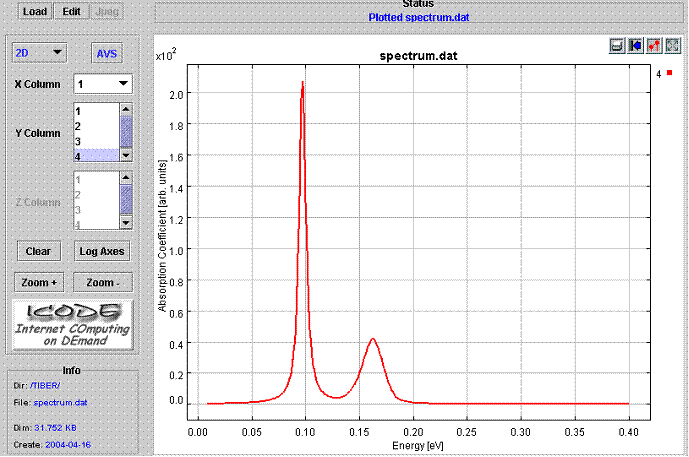
spectrum.dat, which contain the absorption spectum [arbitrary units] of the nanostructure in the following format
|
Energy [eV]
|
TE
|
TM
|
(TE+TM with lorentian smoothing
of 5 meV)
|
Figure 5 shows the calculated spectrum. The picture shows the calculated absorption spectrum of the interband transition between the first 2 levels and 3rd ,4th,5th, and 6th levels (see Fig. 4) of the strained Si/Si0.5Ge0.5/Si quantum well of Fig. 3.
|
|
Fig.5. Plot of the Spectrum file. |
The Control section is used to define general control flags. It will updated in thefuture. For the moment only the block_band flag will affect the output of the simulator.
block_band flag
When selected, the simulator will print out the bulk band structure for each of the block of layers forming the nanostructure. The data are stored in the file bands.xxxx where xxxx correspond to the number of the layer which is always chosen in the middle of the block. The data are stored for this direction L - Gamma - X. Format is:
Bands.xxxx
|
sign*|(kx,ky,kz)|
|
E(8th valence band)
|
E(7th valence band)
|
...
|
E(1st valence band )
|
E(1st conduction band)
|
...
|
E(12th conduction band)
|
where sign = -1 for L-Gamma direction and it is 1 for Gamma-X direction
After the job has been submitted you can monitor the job execution by clicking on the Jobs Status link in the left frame, just above the list of the Services (simulators). For details on this see the relative documentation: Job Monitor Utility.
Results of the simulation can be either downloaded on the CLIENT computer or plotted using the ICODE Hyperplotter tool. For reference see the relative documentaton file: Hyperplotter Graphic Utility.