

Hetero
Tight-Binding based calculation of tunneling in Heterostructures
Welcome to the Tight-Binding Simulator of tunneling in Heterostructure: Hetero !
HETERO is an atomistic tight-binding based simulation tool for the calculation of tunneling properties in heterostructures.
From now on, Client is the computer where you are running the browser (your local computer) while Server is the computer where you are connected (ICODE server).
There are 5 simple steps to follow for a complete device simulation. These are:
- Login
- Select working directory
- Define the simulation parameters
- Monitoring the job execution
- List and description of the files
- Plot the result
HETERO makes use of Empirical Tight-Binding (ETB) approach to describe materials constituents of a heterostructure. An atomic representation is to be given for each material layer, according to the lattice structure and to the cell parameters. The ETB parameters, regarding the on-site energies and the TB couplings between orbitals of the chosen TB basis, are to be defined for all the materials and the interactions relevant to the heterostructure under exam. Finally, a band shift is applied to reproduce the correct band discontinuity at the interface between different materials.
The detailed manual for the HETERO Simulator can be found below in attachment.
Further documentation on the theoretical methods used in the simulator can be found in:
M. Staedele, F. Sacconi, A. Di Carlo, and P. Lugli
Enhancement of the effective tunnel mass in ultrathin silicon dioxide layers
J. Appl. Phys. 93, 2681 (2003).
M. Staedele, B. R. Tuttle, and K. Hess
Tunneling through ultrathin SiO2 gate oxides from microscopic models
J. Appl. Phys. 89, 348 (2001).
A comprehensive introduction to Empirical Tight-Binding modelling can be found in
Aldo Di Carlo
Microscopic theory of nanostructured semiconductor devices: beyond the envelope-function approximation
Semiconductor Science and Technology 18, R1-R31 (2003).
In the present version the tool implements the models of two kinds of pre-defined structures whose atomic basis and TB parameterization have been already previously determined:
- the MOS (Metal Oxyde Semiconductor) system, made by a Si/SiO2/Si heterostructure;
- the Resonant Tunneling Diode (RTD), constituted by GaAs/AlGaAs or GaN/AlN heterostructures.
Anyway, users can define their own input and stucture files, containing a chosen set of Tigh-Binding parameters and a description of the atomic structure (see HETERO Manual in attachment).
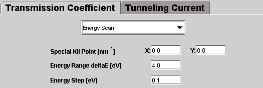
For both the MOS and RTD structures the simulation code allows one to calculate Transmission Coefficient and Tunneling current through the heterostructure.
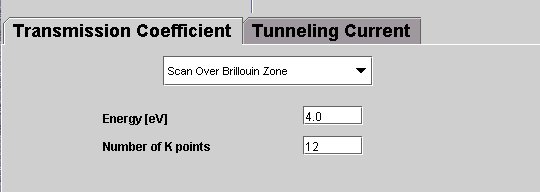
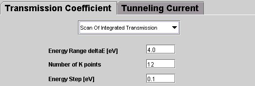
Regarding calculation of Transmission Coefficient T, three different modes of operation are available:
-
Calculation of T as a function of energy, for a given single k|| point in the 2D Brillouin zone.
-
Calculation of T as a function of energy, with T being integrated on the whole 2D Brillouin zone.
-
Calculation of T for a fixed energy value and for a grid of k-points: in this way a picture of the transmission in the first 2D Brillouin zone can be obtained.
As for tunneling current, I/V characteristic is obtained in output, depending on the applied voltage between the two terminals of the system. To this aim, it’s necessary to choose a correct value for the quasi-Fermi levels in the two layers corresponding to the terminals. This value is determined by the doping concentration in the semiconductor.
It must be noted that, as a rule, in RTDs the Fermi level is placed, in both the terminals, inside the conduction band. In this way a degenerated n-doping is assumed, which models the metal contacts.
As for Si/SiO2/Si system, the simulator allows the calculation of the tunneling current when a negative bias is applied to the gate terminal of the MOS diode. In this case there is no n-channel formation in the MOSFET, since it is in condition of depletion or holes accumulation (OFF-state) and the leakage current through the gate oxide assumes great importance for the device performance.
In an n-channel MOSFET the Si substrate is p-doped and the Fermi level will be placed consequently according to the doping. The gate, which in real devices is usually made by polysilicon, is modelled here by a deeply doped Si layer, so that Fermi level lies just above the conduction band bottom.
Step 1 & Step 2: Login and Select working directory
For the first two steps see the detailed instructions in the documentation file: Accessing ICODE system.Step 3: DEFINE THE SIMULATION PARAMETERS
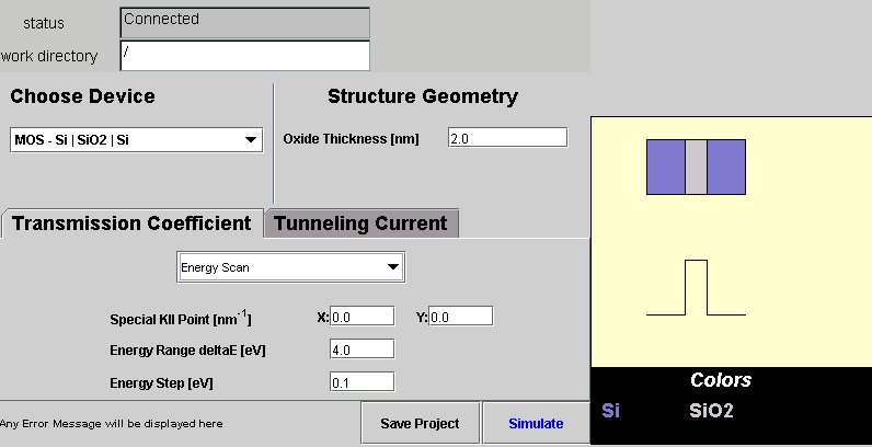
After login and selection of your working directory, you are ready to choose the simulation tool: click on HETERO in the Device simulators frame and the simulation interface opens in a new window.
|
|||
|
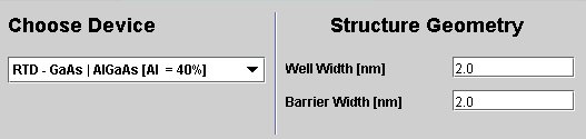
On the top of the frame you can find two text fields: Status and Work Directory. Status: shows the status of the connection with the ICODE server and, when present, the messages about requests to the server, such as the submission of a simulation or save of the project. Work Directory: shows remote working directory of the user In the leftmost menu (Choose Device) you can select one of the three device structures available for simulation : |
|||
|
|
||
It’s worth to note that, in all the following input procedure, the user will be given information about the correct input range by the interface itself. In fact, text messages in the lower left corner will give warnings in case of input out of range and will not allow neither saving of the project nor running of the simulation. In general any error message will be displayed in this position.
On the right, in Structure Geometry the geometrical description of the device can be defined, that is:
For MOS, enter the oxide thickness value, in nanometers.
For RTD, enter the well and the barrier thickness, in nanometers.
The rightmost part of the frame shows a sketch of the chosen structure, which is updated in real time according to the input data. The same is also for the conduction band profile of the device, which is plotted below. Here, the quasi-Fermi levels of the contact layers are shown, as they are entered by the user.
In the lower part of the frame, you can enter the parameters for the simulation.
Click on Transmission Coefficient or Tunneling Current to select one of the two procedures of calculation.
Transmission Coefficient T
Transmission coefficient calculation can be performed in three ways:
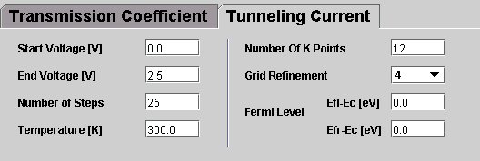
Tunneling Current
If your choice is to perform the Tunneling Current calculation, then this is the frame which will be displayed:
|
|
|
The simulation parameters to be entered in this case are :
- Start and End of the voltage range (in Volt) to be applied to the heterostructure;
- Number of voltage steps for the simulation, to control the level of resolution of the IV results.
- Working Temperature of the device (in K)
- Number of k points: necessary for the Brillouin zone integration. The higher the value , the heavier will be the computational task: so be sure to be careful with it. The minimum allowed value is 2, but a value between 6 and 10 has been found to be reasonable.
- Grid refinement. This input is requested only with RTD structures. In this kind of simulation a more sophisticated, adaptive grid is used for the calculation of integrated transmission. This parameter controls the required level of refinement of the grid; it might be necessary a high value of the parameter to get a correct picture of the current resonance peaks in RTDs. On the other hand, the effect on computational burden is exponential, so we put the maximum value to 6, which is sufficient in most cases.
- Fermi levels. As explained before, the calculation of current requires to set Fermi levels in left (Efl) and right (Efr) contact layers. These have to be expressed in eV, with respect to the bottom of conduction band (Ec): a positive value will correspond to a degenerate case, a negative value to a non-degenerate one.
When all the required input parameters have been entered, two choices are possible:
|
|
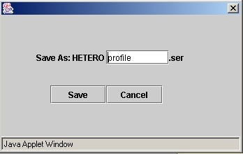
1) You
can save this input configuration in a template file, which will allow
you to run the simulation with this set of parameters in the future,
without re-entering the settings.
Click on Save Project: a window pops up, where you can give a name and save the project in a file with extension “.ser” |
|
|
|
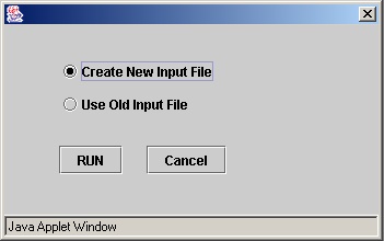
2) You can run the simulation now: click on Simulate.
Now you choose Create New Input File if you want to run a simulation based on the settings entered through the interface. Otherwise select Use Old Input File if you want to use an input file already present in the work directory: in this case the interface settings will be ignored. Finally, click on RUN button to run the simulation or Cancel to abort the submission of the job. |
|
Step 4: Monitoring the job execution
After the job has been submitted you can monitor the job execution by clicking on the Jobs Status link in the left frame, just above the list of the Services (simulators). For details on this see the relative documentation: Job Monitor Utility.Step 5: List and description of the files
Now if you look at the current working directory, in the main FileManager window, the following files should be present (remeber to click on the Reload Page button to refresh the directory list. To have a full description on how to use the FileManager see here):
hetero.in: input file used by current simulation, as it is created by the interactive interface. If you wish to use your own input file, you should give it the name “hetero.in “, then run the job from the interface window, with the option Use Old Input File.
Hetero* .ser: this is the file created by the Save project option, which contains all the parameters regarding a particular device simulation. At any moment you can recall the saved project by clicking on the start link beside the file.
Hetero*.o###, where ### is the number which identifies the job. This file contains the standard output of the simulation program.
Hetero*.e###, where ### is the number which identifies the job. This is the standard error of the simulation program; any run-time error will be shown here.
Output files
If the simulation succeeds, the results are saved in the following output files, identified by the extension .dat.
TE.dat
is a 2 column ASCII file showing the result of Transmission Coefficient Calculation with Energy scan option. The format is
|
Energy (eV)
|
Transm.Coeff. (adimensional)
|
TE_int.dat
is a 2 column ASCII file showing the result of Transmission Coefficient Calculation in the case Scan of Integrated transmission option. The format is
|
Energy (eV)
|
Transm.Coeff. (adimensional)
|
TE_matrix.dat
is a 3 column ASCII file, showing the result of Transmission Coefficient Calculation in the case Scan over Brillouin zone option. The format is
|
kx(nm-1)
|
ky (nm-1)
|
Transm.Coeff. (adimensional)
|
IV.dat
is a 2 column ASCII file showing the result of Tunneling Current calculation. The format is
|
Voltage (V)
|
Current Density (A/cm2)
|
Only the output file for the relevant kind of simulation should be present in the work directory.
Step 6: Plot
Results of the simulation can be either downloaded on the CLIENT computer or plotted using the ICODE Hyperplotter tool. For reference see the relative documentaton file: Hyperplotter Graphic Utility.
| Attachment | Size |
|---|---|
| hetero_manual.pdf | 208.28 KB |